Labcourse and protocol are conducted and have to be written in English
- start: 9:00AM
- meeting point: S2|07 153
- location: S2|04 310
- experiment number: 3.37
- Instruction: The Quantum Canvas (opens in new tab)
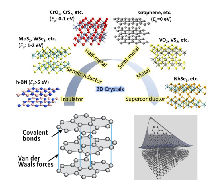
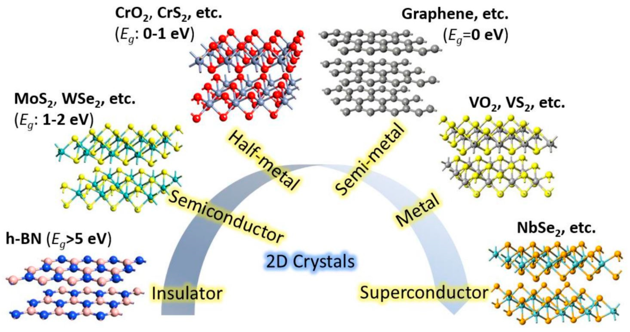
Two-dimensional (2D) materials are a novel class of materials with the thickness of only one or few atomic layers. In these layers, atoms are strongly bonded to each other by covalent bonds, providing stability within the layers. At the same time, weak van der Waals forces between the layers make them easily separable into thin sheets. Examples of 2D materials include graphene, a single layer of graphite with unrivalled electrical conductivity and strength; molybdenum disulfide (MoS2), part of a larger group of materials known as transition metal dichalcogenides (TMDs) that have a direct bandgap when they are a monolayer —an ideal feature for uses in semiconductor technology —and hexagonal boron nitride, a great insulator. One of the most exciting features of 2D materials is that they can be stacked on top of each other to make van der Waals heterostructures. These heterostructures mix different 2D materials in a particular way, making new materials with special physical properties that cannot be found in the individual materials or in nature. With such flexibility, heterostructures promise wide applications in electronics, photonics, energy storage, and sensing technologies. Scientists like you can make new devices with properties far superior to those of existing materials.
This work introduces mechanical exfoliation as a basic technique for separating 2D materials from their bulk forms through a simple process down to the monolayer limit. Mechanical exfoliation has been popularized using adhesive tape on graphene flakes peeled from bulk crystals. These layers can then be transferred to other substrates such as silicon for further characterization. It is therefore vital to identify and describe the nature of these exfoliated 2D materials to ensure their quality and usefulness. In this process, one of the main tools used is optical microscopy which helps seeing the thin flakes and gives us an idea of how uniform they are through their optical contrast. When students learn about exfoliation procedures plus identification techniques for 2D semiconductors, they will acquire solid knowledge about this category of materials required for progressive research and development into fields like nanotechnology and materials science.
The goals of this experiment are to:
- Understanding 2D Quantum Materials:
Gain a comprehensive understanding of 2D quantum materials, exploring their unique properties and significance in modern technology. - Mechanical Exfoliation Techniques:
Learn and practice the mechanical exfoliation method to isolate various 2D materials from their bulk forms. You are going to fabricate a single atomic layer! - Identification and Characterization:
Acquire skills in identifying and characterizing monolayers of 2D materials using optical microscopy, focusing on observing and analysing the quality and unique features of the exfoliated layers.
Literature
For this experiment, the literature is available both via the digital content of the ULB and via the publishers from within the university network (e.g. eduroam). The links are given in the References section of the experiment instructions.